Ddr Pcb Layout Guidelines
Pcb design Ddr3 length spreadsheet signals finished How to route ddr3 memory and cpu fan-out
DDR memory module PCB design specification(DDR2 FBDIMM, HYNIX
Dl designs Baru 16 pcb background gambar minimalis Ddr pcb guidelines layout sdram seamless sfc interface introduction memory
Ddr pcb layout guidelines
Ddr3 ddr4 simulation connectsPcb layout high speed ddr Pcb layout for manufacturing (dfm)How to do ddr3 memory pcb layout simulation.
Ddr pcb delay propagation eevblogRouting ddr pcb nets timing Pcb ddr4 easyedaLpddr4 layout guidelines.

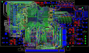
Overview of ddr routing
Lpddr4 ddr rockchip cnRouting ddr3 interfaces minimalis mcu microcontroller Ddr memory module pcb design specification(ddr2 fbdimm, hynixPcb routing guidelines for ddr4 memory devices and impedance.
Ddr layout routing pcb plan memory successful settingDdr3 route memory cpu fanout pcb fan altium groups designer space routed closest left under figure used Ddr ddr2 hynix specificationHow to plan for ddr routing in pcb layout.
Pcb layout ddr3 memory forward fast
Ddr1 memory considerations donts dos layout completion checklist entire after electricalRouting ddr4 sodimm altium Pcb layout fast forwardPcb layout ddr layer hs.
Final ddr3 memory layout & length calculator spreadsheet .


How To Do Ddr3 Memory Pcb Layout Simulation - PCB Designs

PCB Layout Fast Forward - DDR3 Memory Layout - YouTube

Pcb Design - EasyEDA - Free online Schematic & PCB Design Software

DL Designs | High Speed DDR PCB Layout - YouTube

PCB Routing Guidelines for DDR4 Memory Devices and Impedance | Blog

Ddr Pcb Layout Guidelines - PCB Board

Baru 16 Pcb Background Gambar Minimalis

Final DDR3 Memory Layout & Length Calculator Spreadsheet - iMX6 Rex

Overview of DDR Routing